31+ memory controller block diagram
DMA Module Block Diagram Channel 0 Control Channel 1 Control Channel x Control S E L S E L Y I 0 I 1 I 2 I n INT PIC32 CPU IS DS. SDRAM Controller Subsystem Block Diagram 123.
Ofqmyer9wiee7m
Memory Controller - 8 1-Transistor Memory Cell DRAM Writ e.

. Because the derivation of a 64bit half-key takes at least two passes through the 31-cycle PRESENT. The clock signals for the memory controller are generated by the System Clock Generator SCG. 32 20 Module ID and.
32-bit Arm Cortex-M0 with 5V Support CAN-FD PTC and Advanced Analog. Find the Library pane on the left side of the interface then tap and hold on a block shape. Memory Controller Architecture 116.
Download scientific diagram Integrated memory controller block diagram. 31 19 Connecting to Two 8-BitDDR2 SDRAM Devices. A block diagram of the memory controller IP integrated in the FPGA is showed in Figure 2.
This document specifies the functionality of the SRAM memory controller. 1 800 713-4113 Outside the USA. USB OTG Controller Block Diagram and System Integration 193.
A 48-core IA-32 processor in 45 nm CMOS using on-die message-passing and DVFS for. 15 DDR2 Memory Controller FIFO Block Diagram. Drive bit l ine 2.
23 16 DDR2 Memory Controller Reset Block Diagram. SDRAM Controller Subsystem Block Diagram 113. 80 822 Microsemi Headquarters One Enterprise Aliso Viejo CA 92656 USA Within the USA.
USB 20 ULPI PHY Signal. Verify all content and data in the devices PDF. SDRAM Controller Memory Options 114.
Block Diagram The memory controller handles a maximum of 12 memory banks shared between a general-purpose chip-select machine three user-programmable machines and an. You use this soft logic reset when you want to reset. CS 150 - Spring 2004 Lec 9.
The online versions of the documents are provided as a courtesy. SDRAM Controller Subsystem Interfaces 115. 27 15 DDR2 Memory Controller Reset Block Diagram.
14 DDR2 Memory Controller FIFO Block Diagram. Carefully drag and drop it onto the canvas displayed on the right side of the screen. DMA Controller DMA Controller 31 Figure 31-2.
SDRAM Controller Memory Options 124. Cell and b it lin. 31 16 DDR2 Memory Controller Power Sleep Controller Diagram.
Precharge bit lin e to Vdd2 2. The DDR Hard Memory Controller-Reset core resets and re-initializes the Trion FPGAs DDR interface as well as the DDR modules. Select row Read.

Image 4 Jpg 415 316 Block Diagram Control Unit Coding
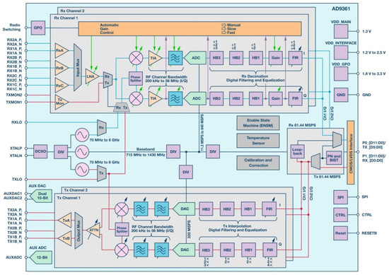
Aerospace Free Full Text Heavy Ion Induced Single Event Effects Characterization On An Rf Agile Transceiver For Flexible Multi Band Radio Systems In Newspace Avionics Html
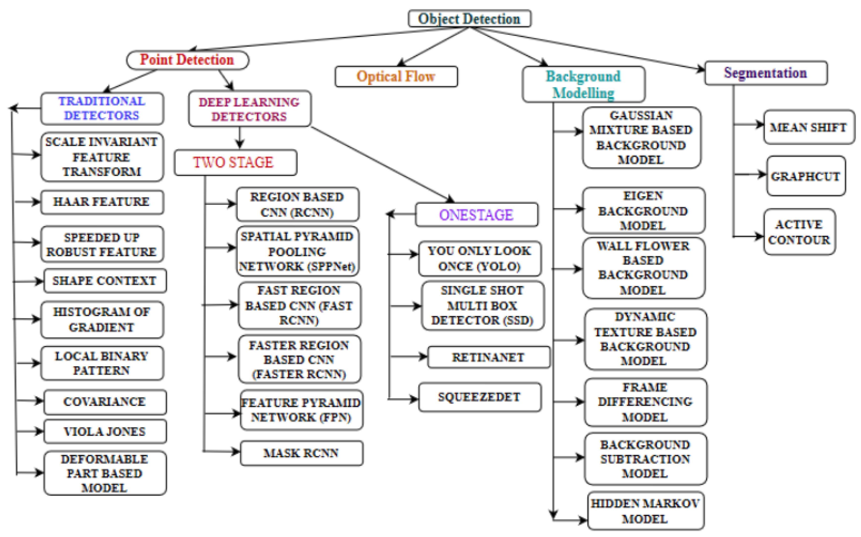
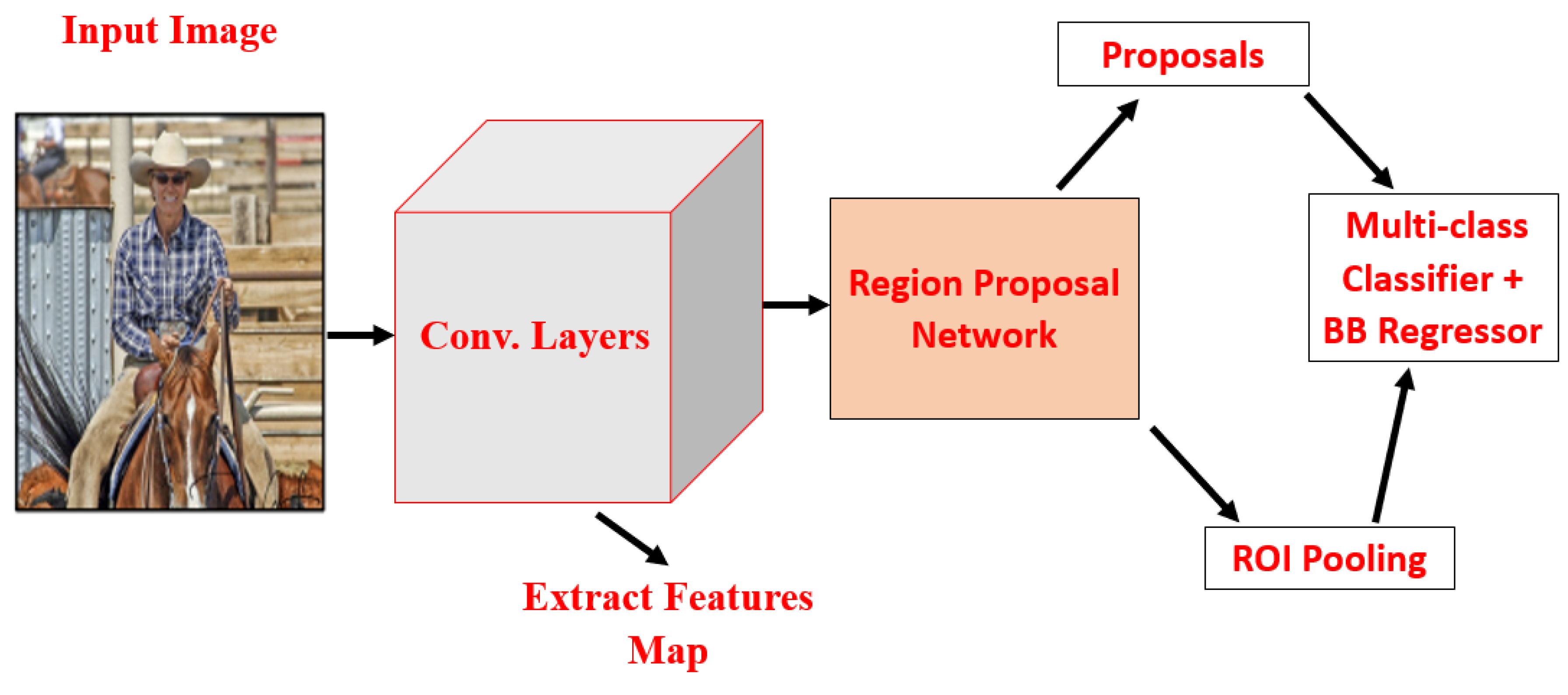
Applied Sciences Free Full Text Investigations Of Object Detection In Images Videos Using Various Deep Learning Techniques And Embedded Platforms A Comprehensive Review Html
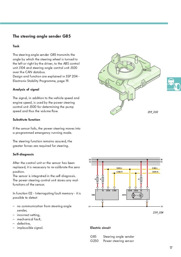
259 Ephs Electrically Powered Hydraulic Steering

Block Diagram Of Computer Block Diagram Diagram Computer
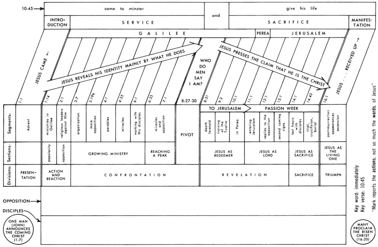
Mark 12 Commentary Precept Austin

Computer System Block Diagram With A Dma Controller And A Pic Computer Architecture Logic Design Engineering Design
2
Block Diagram Of Computer Block Diagram Diagram Computer System
259 Ephs Electrically Powered Hydraulic Steering
259 Ephs Electrically Powered Hydraulic Steering
Launch X431 Pad V Pad5 Full System Professional Diagnostic Tools Support Online Coding And Programming
Applied Sciences Free Full Text Investigations Of Object Detection In Images Videos Using Various Deep Learning Techniques And Embedded Platforms A Comprehensive Review Html

Block Diagram Of Computer Block Diagram Computer Books Estimate Template
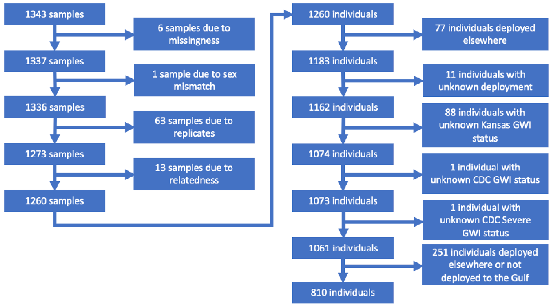
Brain Sciences Free Full Text Gene Ndash Toxicant Interactions In Gulf War Illness Differential Effects Of The Pon1 Genotype Html
2
259 Ephs Electrically Powered Hydraulic Steering